While one- and multidimensional defects are conventionally being avoided, we demonstrate that their selective use can lead to a strong enhancement of piezoelectric and dielectric properties. Moreover, their stability can help to extend the operating limits of our electronic devices.
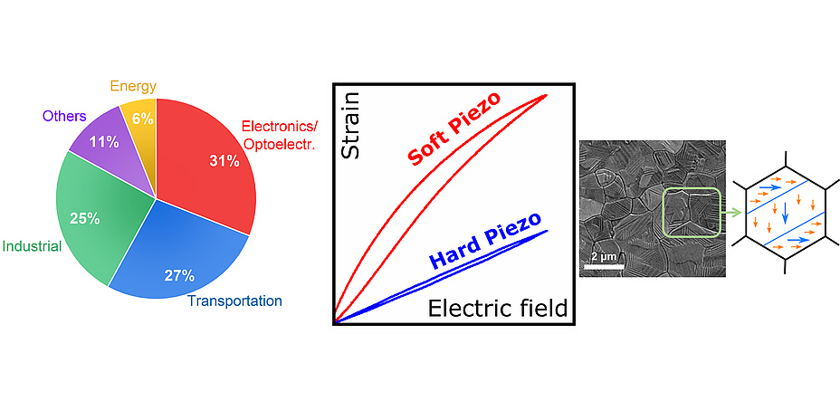
Piezoceramics have the unique ability to convert mechanical signals into electrical ones and vice versa. This property made them indispensable in many everyday devices, such as sensors, actuators, miniature motors, and ultrasonic transducers (Fig. 1a). Moreover, they are becoming increasingly important parts of emerging technologies in consumer electronics, autonomous vehicles, Internet of Things, medical robotics, and in-body sensors. Recently, they were predicted to be the fastest growing segment of the electroceramics market [1], which was accelerated by their increased use during the pandemic (e.g., in ultrasonic welding of face masks).
Since most piezoceramics are also ferroelectric, the dynamics of ferroelectric domains contributes decisively to their macroscopic response. Historically, researchers have strived to prepare these materials in a single-phase form with uniform microstructures. The only appreciated defects were acceptor/donor dopants (0D defects), which allow controlling the movement of domain walls (Figure 1b,c); increasing the movement increases the strain (soft piezoceramics for actuators and sensors), while clamping the domain walls reduces the losses (hard piezoceramics for highfrequency applications, e.g., transducers). On the other hand, one- and multidimensional defects such as dislocations and secondary phases have always been considered as culprits. However, in real piezoceramics, they can hardly be avoided completely. So why not use them to our advantage?
The typically-used piezoceramics have a perovskite crystal structure and can thus be described as ferroelectric and ferroelastic. This means that the motion of the domain walls is affected by both electric fields and mechanical stress. However, clamping the domain walls externally using these stimuli is impractical. It would therefore be more efficient if the clamping could originate from the sample´s own microstructure, e.g., from a defect “sitting” in the piezoceramic matrix (Figure. 2a,b). To achieve this, we introduced ZnO inclusions [2], which have previously been shown to increase material´s depolarization temperature [3]. The different thermal expansion of these 3D defects imposed thermal stress on the matrix grains, while their non-ferroelectric behaviour rendered them rigid during electric field application [4]. Moreover, the charge separation in the semiconducting ZnO additionally pinned the domain walls at the semiconductor/piezoceramic boundaries. Both effects resulted in reduced domain wall movement and a twofold reduction in mechanical and piezoelectric losses, which is crucial for high-frequency applications.

Figure 2: Piezoelectric hardening by secondary phases (a). ZnO inclusions inpiezoceramic Na1/2Bi1/2TiO3-BaTiO3 (inset was taken using piezoresponse force microscopy) (b) and CaTiO3 precipitates in piezoceramic (Ba,Ca)TiO3 (c) [2-4]. Scanning and transmission electron microscopy.
Although ZnO inclusions interacted with domain walls, their positioning enabled only domains located near the boundaries to be pinned, while those positions inside the matrix grains remained unaffected. A homogeneous distribution of the secondary phase within the piezoceramic grains would have been much more desired. However, this is not easily achieved with conventional ceramic processing. To solve this problem, we “borrowed” an approach from metallurgy. Precipitation hardening is an established method for increasing the yield strength of metals, whereby precipitates are formed by annealing a supersaturated solid solution. We selected the piezoceramic system (Ba,Ca)TiO3, which exhibits a curved line of solid solubility in its phase diagram. The material was first sintered at high temperature in the singlephase region (high solubility of Ca in BaTiO3) and subsequently quenched to preserve this state. The supersaturated solution was then aged at an intermediate temperature, forming non-ferroelectric CaTiO3-rich precipitates in the piezoceramic BaTiO3-rich matrix (Fig. 2c). The precipitates pinned the domain walls and thus reduced the losses [5].
3D defects are not the only microstructural imperfections that can be used to our advantage. An even stronger interaction can be expected when the defect size is reduced below the domain size, i.e. to the range of a few nanometres. Example are 1D linear defects called dislocations. While dislocation movement is one of the fundamental mechanisms in metals, they have not attracted much attention in ceramics. However, dislocations in ionic materials are expected to exhibit not only strain fields but also a charged core and an associated space charge layer (Figure 3). Thus, they offer an easy way to introduce local mechanical and electric fields into the microstructure. The main challenge is to introduce a sufficiently large dislocation density into brittle oxides. We have demonstrated that dislocation networks can be imprinted either by room-temperature plastic deformation (in KNbO3 [6]) or by high-temperature mechanical creep (in BaTiO3 [7]). Interestingly, the dislocations pinned the domain walls and hardened the piezoelectric at low applied electric fields, but got depinned at higher electric fields and caused a mechanical restoring force that returned the domain walls to their original position. This led to a huge increase in the piezoelectric coefficient from 100 pm/V in undeformed samples to 1890 pm/V in samples with dislocation networks [7] (Figure 3c). In addition, the permittivity increased from 170 to 5810.

Figure 3: a) Charged dislocation with space charge layer and elastic strain field. b) TEM image of a slip band with edge dislocations in deformed KNbO3. Inset shows the image of the deformed sample. Courtesy M. Trapp and M. Höfling. [6] c) Giant increase of piezoelectric coefficient and permittivity in deformed BaTiO3, after depinning of domain walls at large E-fields [7].
These examples demonstrate that 1D and 3D defects can be used to tune the functional properties of electroceramics. A major advantage over 0D point defects is their thermal and electric field stability, which allows their use under severe drive conditions. Remaining challenges include simplification of the processing steps, extension to other piezoelectric systems, and detailed investigation of the underlying physical mechanisms.
Acknowledgements:This work was carried out in the Division Nonmetallic-Inorganic Materials (Head: Rödel) at TU Darmstadt with the financial support of the Deutsche Forschungsgemeinschaft (DFG) and the AYI programme of TU Darmstadt.
References:
- Gagliardi, Am Ceram Soc Bull 2017, 96, 27.
- Lalitha et al., Appl Phys Lett 2017, 111, 022905.
- Zhang et al., Nature Comm 2015, 6, 6615.
- Riemer et al., Acta Mater 2017, 136, 271.
- Zhao et al., Adv Mater 2021, 33, 2102421.
- Höfling et al., J Eur Ceram Soc 2021, 41, 4098.
- Höfling et al., Science 2021, 372, 961.
Jurij Koruza obtained his PhD at Jožef Stefan International Postgraduate School, Slovenia, in 2013 and was a group leader at the Department of Materials Science at the Technical University of Darmstadt, Germany, until 2021. Since September 2021 he has held a tenure-track position at the Institute for Chemistry and Technology of Materials at TU Graz. His research is focused on the development of new electroceramic materials.