Radiation Damage in Microelectronics
This includes ionising radiation stress, which affects device characteristics, leading to circuit degradation. Investigating such problems, as well as irradiation campaigns with custom integrated circuits (ICs) are the day-to-day focus of the team at the Institute of Electronics.
Analog IC design is an integral part of microelectronics. Designers have a host of options when it comes to meeting specifications, they need to make decisions on trade-offs between different parameters, and also need to comply with strict requirements in terms of precision, fast timing and low noise. It becomes even more challenging when reliability issues, such as ionising radiation stress, come into play.
It is this combination that makes research into radiation-hard integrated circuit design so exciting. Ionising radiation changes the electrical characteristics of microelectronic devices. As a consequence, instruments for medical and industrial X-ray imaging, space or high-energy physics have to be qualified and potentially hardened against ionising radiation.
Origins of ionisation damage
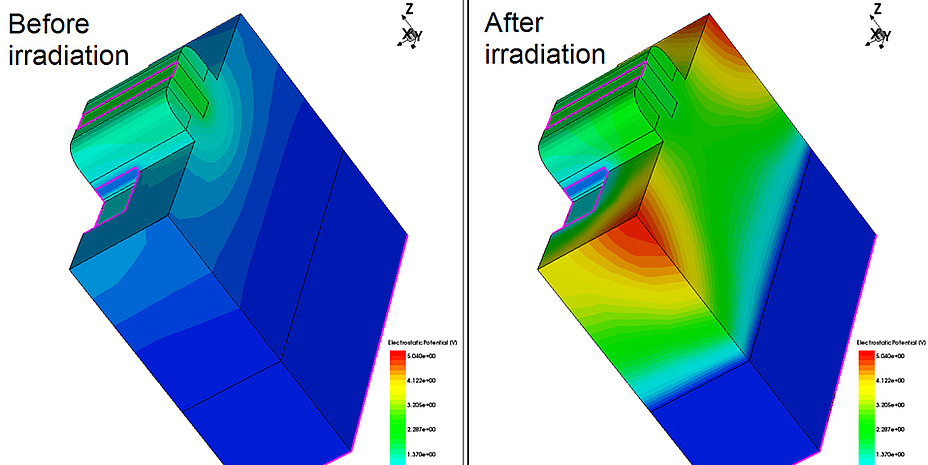
Exposing ICs to X-rays or gamma rays causes ionisation, resulting in randomly generated free charge carriers across the structure. Every IC consists of a bulk semiconductor and interleaved layers of metals and insulators. Free charge carriers in the conducting layers can be easily collected. Unless it is generated by energetic particles, the resulting current is negligibly small. In the case of insulator layers, an X-ray photon leaves behind a number of electron-hole pairs. Holes in particular have extremely low mobility, but electrons can escape the interaction region and move towards conductive layers more easily. Meanwhile, holes remain as net positive charge trapped in the insulator, producing a parasitic electric field. This effect is particularly undesirable when the insulator region is adjacent to a device, for example the gate oxide of a metal-oxide-semiconductor (MOS transistor. Even a low radiation flux can accumulate to a significant net charge after receiving a certain dose. Parasitic electric fields in the gate oxide cause the threshold voltage of an MOS transistor to shift (see Figure 1), while leakage current also increases and the intrinsic gain degrades; these are just a few of the possible effects.
In modern complementary metal-oxidesemiconductor (CMOS) ICs, the gate oxide, measured by the number of atomic layers, is so thin that the trapped oxide charge is neutralised by means of the tunnelling effect. In these modern processes, transistors are separated from each other by a much thicker insulator – this is known as shallow trench isolation (STI). After exposure to X-rays the STI is rich in trapped charge that has a strong influence on a device’s characteristics. For example, a parasitic transistor is formed along the gate edge (see Figure 2), leading to off-state leakage currents. With MOS transistors, one way to counteract this problem is to use edgeless or enclosed layouts, where the STI edge only sees the outer terminal, meaning there is no potential path for the leakage current. However, this solution cannot be used with narrow transistors; it also does not comply with the design rules of some semiconductor foundries, in particular in sub-65 nm nodes. Taking these factors into account, as well as requirements for devices other than MOS, new solutions for device geometry and the circuit topology level are urgently required to raise radiation tolerance limits.

Figure 2: Experimental results: absolute threshold voltage shift of N-type MOS transistors with different layouts and same equivalent channel dimensions as a function of the total ionising dose (TID).
Cotomics and robustic projects
Our group at the Institute of Electronics is currently involved in several projects dealing with the radiation hardness of ICs. The precursor was the recently completed Cotomics project, which evaluated radiation tolerance and explored hardening strategies for a broad variety of devices in the 180 nm CMOS production process. It targeted reliability improvements in next-generation computed tomography. One of our current projects, RobustIC, is investigating the combined impact of ionising radiation, overvoltage and temperature effects, looking into new custom devices as well as circuit solutions. As a consequence of these two projects, in the last four years we have designed four integrated circuits with a huge number of devices and test circuits for radiation tolerance characterisation. So far, our results have been based on seven irradiation campaigns using a 10-200 keV X-ray tube beam (see Figure 3). For each experiment, the total ionising dose received by the circuit had to be determined at each characterisation step. We were able to calibrate the dose between three different facilities using several dosimetry techniques, in collaboration with experts from MedAustron, Seibersdorf Laboratories, CERN-EP and the Institute of Solid State Physics.

Figure 3: Formation of a radiation-induced parasitic channel by charge trapped in STI along the gate of a standard linear MOS transistor (N-type).
Initial funding grant
Scaled CMOS processes below 65 nm are attractive for a range of sensing, signal processing and computing applications, but the effects of radiation on individual devices are still not fully understood. In 2018 our group received an initial funding grant from the Advanced Materials Science Field of Expertise to kick off research into radiation tolerance and hardening techniques in 28 nm and 40 nm technology nodes. The new SIRENS project looks beyond medical technologies to the exciting fields of space and high-energy physics instruments, where the amount of energy absorbed over a device’s lifetime as a result of radiation can reach previously unexplored levels.

Figure 4: Exposed silicon die of the Mitigation and Modeling of Radiation Effects (MiAMoRE) IC ready for irradiation.
Kontakt
Alicja MICHALOWSKA-FORSYTH
Dr. mgr inz.
Institute of Electronics
Phone: +43 316 873 7523
alicja.michalowska@tugraz.at
Varvara BEZHENOVA
Dipl.-Ing.
Institute of Electronics
Phone: +43 316 873 7530
varvara.bezhenova@tugraz.at


