TU Graz/ TU Graz/ Services/ News+Stories/

Nanoworld in 3D

06/23/2016 | Planet research | FoE Advanced Materials Science

By Gerald Kothleitner

Gaining detailed knowledge about atomic structure and chemical composition is paramount for a deeper understanding of the properties of matter and their potential applications in technology.

Nanoworld in 3D.
Electron microscopy thus represents a key tool for the comprehensive characterization of materials at highest spatial resolution in three dimensions. Atomic-scale defects already define electronic and optical properties of photonic and semiconducting materials, the location of dopant atoms determines the performance of silicon transistors and spintronic devices and the chemistry and orientation of surfaces and interfaces of metallic particles control their catalytic activity. Richard Feyman´s challenge from 1959, to build a better microscope that allows for an identification of individual atoms in a chemical structure, could be tackled just recently with the realization of aberration-corrected electron microscopes. These sophisticatedly engineered systems consist of lens modules that can resolve object structures smaller than  100 picometer. The Center for Electron Microscopy (ZFE) Graz hosts one of these instruments (ASTEM, Austrian Scanning Transmission Electron Microscope) since 2011 and operates it together with the Institute for Electron Microscopy FELMI at the TU Graz. With its configuration it is one of the most capable and enabling devices for material research world-wide.

Elemental analysis at atomic scale

Element-specificity can be obtained with suitable detectors such as X-ray or electron energy-loss spectrometers (EELS) interfaced to the microscope. In order to properly incorporate and synchronize all physicochemical signals on the ASTEM, much effort went into the correct implementation of software and hardware. Tightly cooperating with the US company Gatan Inc. over many years, an efficient operating environment could be designed that carries the handwriting of the workgroup. With this unique configuration it was for the first time possible to study elemental concentrations on a specific crystallographic lattice site. The work, published in the magazine Physical Review Letters, revealed that the recorded analytical intensities can only be understood by complementary simulations. These calculations are carried out by cooperation partners in theory groups located in Melbourne (Australia) and Tokyo (Japan).
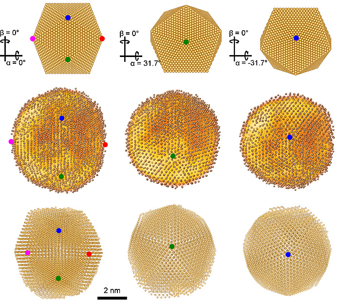
Model, reconstruction and simulation of atomic positions in the nanocluster. Top: Model of a modified icosahedron seen from the top and along two different fivefold symmetry axes. Middle: Rconstruction of atomic positoins seen along the same directions. Bottom: Molecular dynamics simulations. Fivefold symmetry centers are indicated as dots.  

Electron tomography – the third dimension

Three-dimensional diagnostic tools have given insights into the human body, which classical X-ray imaging cannot deliver. In analogy, structural details from a thin and transparent TEM (transmission electron microscopy) specimen sample can also remain obstructed when observed from a single projection only. Approximately 100 years ago, the Viennese Johann Radon laid down the mathematical basis for tomography by showing that a sufficient number of projections taken from different viewing angles enable the three-dimensional reconstruction of an object when subject to an inverse Radon transformation.  Electron tomography in the physical sciences, being experimentally rather challenging, only became popular about 15 years ago. We started our research in this highly dynamic field in 2009. Besides developing new experimental approaches, the workgroup deals with the complex problem of optimizing and adjusting reconstruction algorithms for the respective microscope signals and how to correlate theoretical information with 3D data such  that more physically meaningful information can be extracted from the experiment. This shall be exemplified in two co-operation projects with the Institute of Experimental  Physics at TU Graz and the Institute of Physics at the University of Graz. 

Metallic nanoclusters

A study published in the magazine Nature Communications is dealing with the synthesis and characterization of metallic nanoclusters in superfluid Helium. The issues under question were the growth mechanism, and the structure and chemical composition of these clusters. To answer this, our post-doc Georg Haberfehlner first developed a novel acquisition scheme that minimized image noise and scan distortions. Applying different reconstruction algorithms to the optimized projections then enabled the extraction of atomic positions and the chemical make-up from the obtained core-shell object. From the 3D visualization, valuable conclusions about material properties and possible uses could be derived.
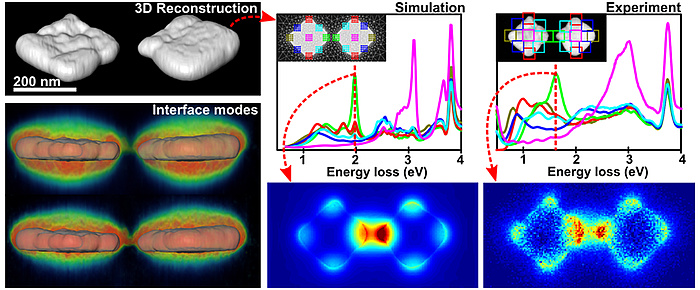
Three-dimensional reconstructions and simulations of localized surface plasmon resonances in coupled silver nano-cuboids.

Plasmonics

Another application for electron tomography lies in the field of plasmonics. Light or electromagnetic radiation is coupled onto nanometer-sized structures (for instance, gold or silver). Depending on shape, size, environment and chemistry of the object, so-called surface plasmons are formed, which are resonances of the metal electrons, responding to the incoming radiation. During the Middle Ages, glass-makers unknowingly used this phenomenon when they produced colored church windows by adding tiny gold particles to the melt. A TEM offers enough spatial and spectral resolution to resolve such modes. Microscope beam electrons, running by these structures in close proximity, loose energy and this can be measured spectroscopically. If this is carried out for each tilt-angle, the full 3D energetic distribution of the modes can be reconstructed and related to theoretical calculations (published in the magazine "Nano Letters"). 

Physical science research

Analytical electron microscopy is a versatile tool in physical science research and offers many ways to characterize exciting materials. The multitude of possibilities require considerable expenditure on equipment, expertise and intense exchange of knowledge with other scientists at an international level. Consequently, the FELMI-ZFE is embedded into an international consortium of 14 toplevel electron microscopy facilities throughout Europe, called ESTEEM, aiming to aggregate microscopy research know-how.

Information

Gerald Kothleitner is head of the working group for analytical transmission electron microscopy and electron tomography at the Institute of Electron Microscopy and Nanoanalysis. His research includes methodological developments for spectroscopic analysis and tomography and their application to problems in materials science.

Contact

Gerald KOTHLEITNER
Ao.Univ.-Prof. Dipl.-Ing. Dr.techn.
Institute of Electron Microscopy and Nanoanalysis
Steyrergasse 17/III
8010 Graz, Austria
Phone:+43 316 873 8336
Fax: +43 316 108336
gerald.kothleitner@felmi-zfe.at